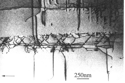
1. Shown below is a bright field TEM image of dislocations in GaAs. Which of the following is dominant in this image: phase contrast, mass-thickness contrast, or diffraction contrast? Why do you think so? Is there any observable evidence that either or both of the other mechanisms also contribute to what we are seeing? If so, explain.
Diffraction contrast dominates, as usual. It is responsible for the fact that we see the dislocations (all the straight and wavy dark lines) at all.
Diffraction conditions change near the dislocation lines because of local bending of the lattice planes. (In this case, for a bright field image, the dislocations apparently lead to areas where the planes are closer to the Bragg condition and diffract much more strongly than in the bulk of the crystal where there are no defects. As a result, since only the directly transmitted electrons are included in the bright field image and the diffracted electrons are excluded, the dislocations appear dark on a relatively brighter background.) There is no chemical difference at the dislocations and no reason to think that the crystal is thicker or thinner there, so mass-thickness contrast does not play a role in the appearance of the dislocation lines. Phase contrast is more applicable on a much finer scale, providing contrast such as periodic lattice fringes, and relies on interference between both direct and diffracted beams. It again does not lead to the dominant contrast features in this image, which are from the dislocations.
There is also some contrast due to mass-thickness effects. This is seen as the change in the overall background intensity, ranging from lighter at the bottom left to darker at the top right. This is presumably because the sample does not have uniform thickness, but is thinner towards the bottom left, leading to less scattering of the transmitted electrons.
You may have thought that the regular, periodic "dots" or cross-hatching in the image were a phase contrast effect. Actually, this is an artifact - a Moiré effect due to printing/copying - and doesn't exist in the original micrograph. Any explanation in terms of TEM contrast mechanisms is therefore meaningless, but I salute your effort if you tried to explain this, and you certainly won't lose any points for the attempt.
2. Determine the depth of field for (a) an SEM and (b) a TEM for imaging at a magnification of 10,000 X in both instruments. Assume that the relevant aperture angle a in each case is 8 mrad. The resolution limit of the SEM is about 70 Å and the resolution limit of the TEM is 5 Å.
for SEM: depth of field = d/Ma - dp/a
- resolution of the eye (d) is about 0.1 mm
- M = 10,000 X
- a = 0.008 rad
- dp = probe size; estimate is that resolution 2 dp, so dp 70 Å / 2 49.5 Å
- depth of field is then = 1.25 µm - 0.619 µm = 0.631 µm
for TEM: depth of field L dlimit / 2a = 0.03125 µm
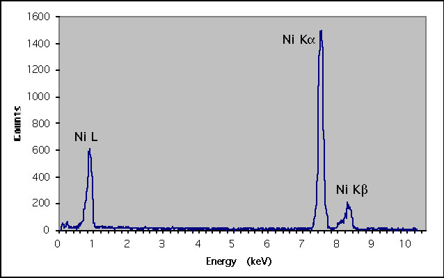
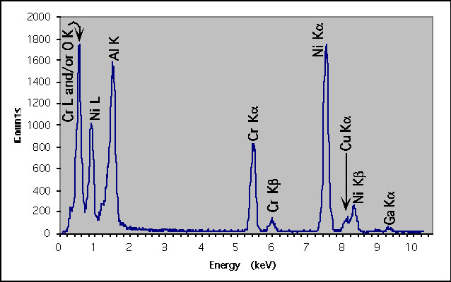
3. Used "NJZ M & M Tools" at the Argonne website to identify the peaks in these EDS spectra (note that peaks are fully labeled here, but as long as you correctly identified the elements from which each peak arose, that was sufficient for this problem). The first spectrum is from an elemental nickel (Ni) particle. The second is from a region that contains Ni, Cr, Al, small amounts of Cu and Ga, and possibly O. (No points deducted for missing the last three, which are all from very minor and/or overlapped peaks. By combining the EDS information with electron diffraction data, it was found that this region was a Ni-Cr-Al-O spinel phase. The Cu arises from the Cu grid upon which the thin specimen was mounted, and small amounts of Ga are implanted into the specimen during preparation by focused ion beam (FIB) techniques.)