SS#_________________________
Grade_____________
MatSE 430
1998 - HW9 - due 5 pm 11/19/98 (with usual grace period)
1. In SEM, the resolution is limited by the size of the electron beam or probe. The Abbé diffraction limit is one constraint, and the spherical aberration of the final lens is also important. The contributions to the beam diameter from these two effects are
The 3rd factor (the "ideal" term) discussed as being important is whether the signal was sufficient. Consider the case of a field emission source for the SEM; here, the brightness is so high that there is sufficient signal, and the ideal term can be ignored. This SEM is operated at 30 kV (lambda = 0.097 Å), and has a spherical aberration coefficient of Cs = 2 cm. Assume that other aberrations, astigmatism, and all other factors are negligible.
a. determine the optimum aperture semi-angle alpha.
b. calculate the minimum probe size that can be obtained
c. estimate the resolution of the instrument, under ideal operating conditions
d. discuss whether the value you calculated in c is reasonable, and compare it to what you would expect for a more typical SEM with a thermionic gun
2. Both the excellent resolution and unusual depth of field are important reasons why SEMs are widely used. In some cases, one would like to have both resolution and depth of field simultaneously, but, unfortunately, there are tradeoffs between the two. Suppose a very irregular specimen is examined in which at least a 10 micron depth of field is required. Also, features of 1 micron size need to be observed. What range of magnifications can be used if the aperture semi-angle is 5 mrad? Assume that a probe diameter of 50 Å is achievable, and remember that what the eye can distinguish on the CRT screen limits the attained resolution.
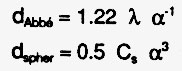
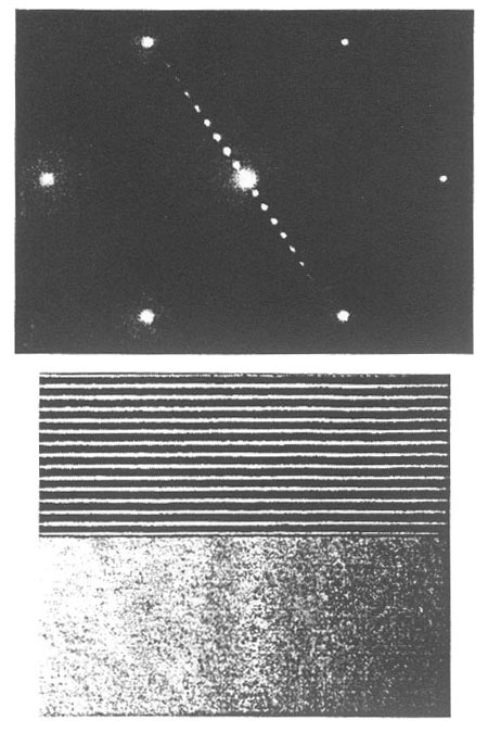
3. The TEM diffraction pattern and BF image below are from a specimen that is a cross-sectional slice of a synthetic multilayer film. The substrate is crystalline Si (F cubic, a = 5.43 Å), and the alternating layers are amorphous W and amorphous Si. Structures of this type can be used as high efficiency x-ray mirrors in applications such as x-ray lithography (in patterning of semiconductor devices), short wavelength lasers, and x-ray telescopes. Note that the orientations of the image and the diffraction pattern are not the same, but no matter in this problem. The camera length for the 72 mm wide diffraction pattern is about 3230 mm, and the TEM operating voltage was 200 kV (lambda = 0.02508 Å).
a. Index the six outer spots in the diffraction pattern from the crystalline substrate. Determine the zone axis direction for the incident beam.
b. From what does the row of closely-spaced spots in the diffraction pattern come? What is the periodicity associated with these?